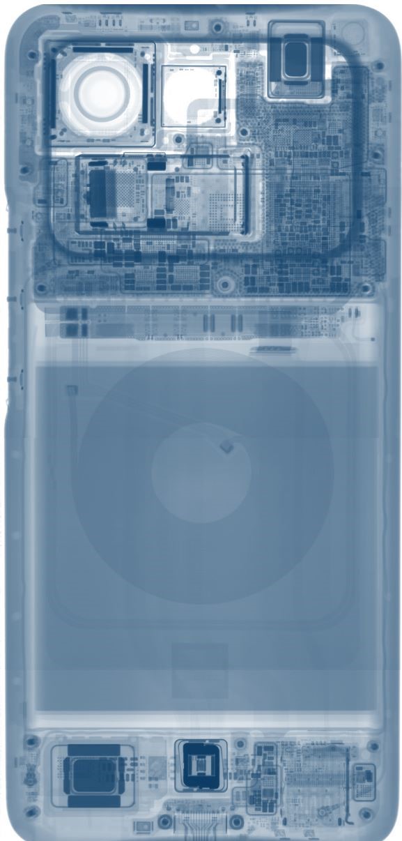


Computed Tomography (CT) is a highly versatile analytical tool that can produce non-destructive 3-dimensional images of objects. This makes it ideal for examining both exterior and interior dimensions, as well as inspecting the internal structures of products, components, and materials without requiring them to be dismantled. CT is often used in the early stages of failure analysis to provide quick insights and clues to the potential root causes of product or material failure. Additionally, CT offers high resolution imaging with resolutions as low as a few microns.
At CarlBerk, we have extensive experience utilizing CT to inspect a wide variety of complex objects ranging from small electronic components such as capacitors, solders, and interconnects, to larger components like batteries and PCB boards. Additionally, we have expertise in inspecting even larger objects such as consumer electronics like cell phones and wearables.
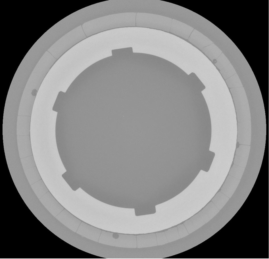
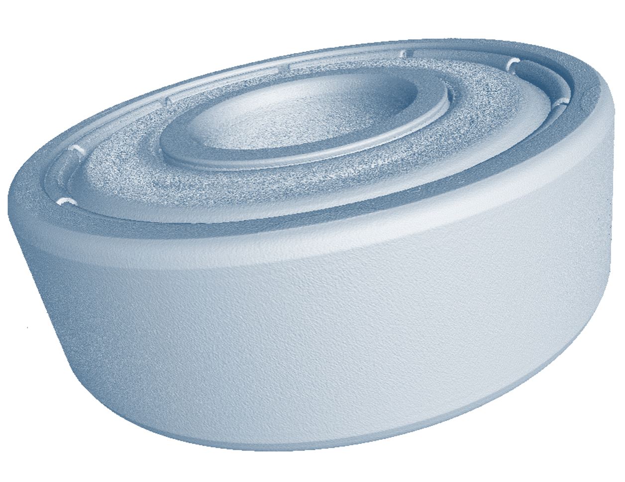
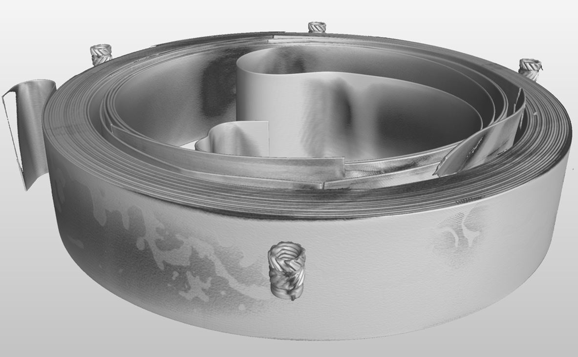
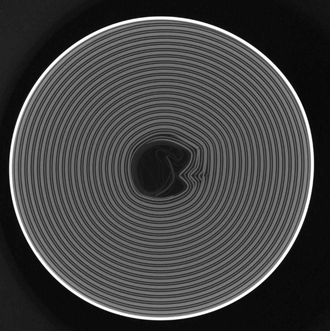
Below are examples showing the benefits of utilizing CT for inspecting materials and/or process defects:
